| Detector type | Housing | Channels | Element size | Diameter (Spot size) | Rel. Sensitive Area | FOV | D* [cm 1) |
| LIM-314 | TO-8 | 4 | 4 mm² (x4) | Ø 8,3 mm | 30 % | 42° | 3.5x10⁸ |
| LIM-222 | TO-39 | 2 | 2 mm² (x2) | Ø 4,9 mm | 41 % | 20° | 4.5x10⁸ |
| LRM-254 | TO-39 | 4 | 2 mm² (x2) | Ø 4,7 mm | 21 % | 55° | 4.5x10⁸ |
Compact pyroelectric detectors based on micro-machined chip carriers
A miniaturized multi channel detector differs in many ways from a more conventional multi-channel detector. For example, it features special chip carriers. The influence of such elements on the performance of these special detectors is clearly illustrated in this technical article.
A. Günther and M. Ebermann
InfraTec GmbH, Gostritzer Strasse 61-63, 01217 Dresden, Germany,
Abstract
A novel micro-machined chip carrier system for pyroelectric detectors was developed that integrates the sensor elements as well as the infrared filters into one assembly. Based on these chip carriers miniaturized multi-channel detectors with attractive electro-optical parameters especially for gas analysis measurements were engineered.
Introduction
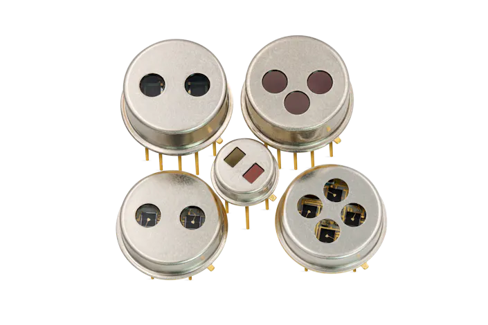
Pyroelectric infrared detectors are a core component of measurement and control devices in industrial safety technology (e.g. monitoring of gas concentrations [1] and flame sensors in industrial plants or mines) as well as in medical sensor technology (e.g. anesthetic gas sensors or emergency medicine). Commercially available sensor models cover one- to four-channel detectors with transistor outline (TO) packages in various sizes. So far, InfraTec GmbH has offered dual-channel detectors in TO39 housing and four-channel ones in TO8. The progressive trend of sensor module miniaturization requires a stronger diminishment of the size of their single components, and a higher integration in smaller housings without a loss of performance. For this purpose a novel micro-machined chip carrier was developed. This chip carrier made from silicon facilitates a significant higher integration of the sensor elements and infrared filters. Therefore, it is possible to minimize the detector package size while the number of channels remains the same, or the number of channels can be increased while the housing remains the same size. Simultaneously, a large active area of the sensor elements and in addition a high field of view (FOV) can be realized. It is even possible to improve those parameters compared to previous solutions. Meanwhile the chip carriers are implemented in their own miniaturized detector family (Fig. 1).
Conventional design of pyroelectric infrared detectors
Pyroelectric detectors are classified as thermal sensors. Their functional principle is based on the pyroelectric effect of the applied sensor material. A change of the detector chip's temperature leads to a change of the materials surface charges that can be converted to an output voltage by an integrated amplifier [2]. Important application-relevant parameters are, besides the specific detectivity, the size of the active sensor element area as well as the FOV.
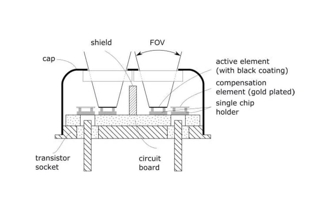
They decisively define the achievable level of the signal-to-noise (SNR) ratio. The applications mentioned above usually work in a frequency range from 1 Hz to 10 Hz. In combination with pulsed thermal emitters the highest SNR can be achieved. Thus, there exist defined requirements on the detector's assembly and packaging techniques along with the hybrid integration of the sensor elements (e.g. made of LiTaO
The active sensor elements are either directly mounted on the circuit board or on a special chip carrier. Compensation elements are added in the same plane and increase the required footprint.
The FOV (for a given size of the detector elements) is limited by the opening in the cap (cap aperture). Due to the typical manufacturing and assembly tolerances no further optimization is possible.
The application-specific infrared filters are adhesive bonded in the transistor cap. Therefore, the mostly sensitive filter coatings are directly exposed to environmental impacts. This could have a negative influence on their long-term stability.
The size of the filters depend on the area of the cap apertures, which may result in higher material costs.
To reduce optical crosstalk between neighboring channels it is necessary to add additional shields that need appropriate space.
Novel modular chip carrier
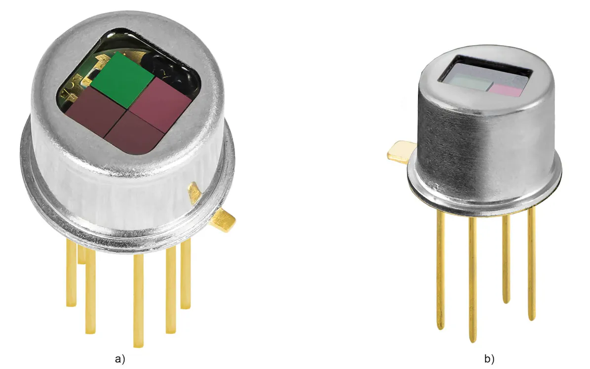
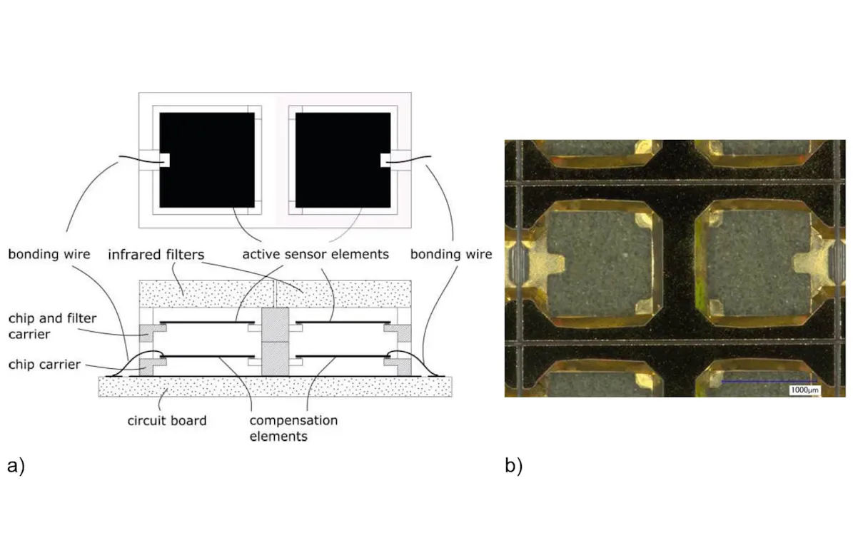
The solution to eliminate the aforementioned disadvantages and to optimize the relevant detector parameters entails a chip carrier that integrates the sensor elements as well as the infrared filters in a compact assembly into the detector housing. Fig. 3 shows the basic concept (a) and a micro-machined chip carrier without sensor elements for a dual-channel detector (b).
The concept has the following characteristics and advantages:
cost-efficient micro-mechanical manufacturing process based on silicon, electrical conductivity due to metallization,
small space requirement (compared to the active area of the pyroelectric sensor elements),
enables the mounting of the infrared filters directly on top of the chip carrier and results in significant reduction of the filter size and material costs,
modular concept, integration of several channels in one part, space saving configuration of compensation elements due to stacked structure,
optimal thermal connection and effective optical shielding of the compensation elements,
low heat dissipation due to minimal contact area for the sensor elements and optimized thickness of the ambient air layers (distance to the filters, the circuit board, and the chip carrier of the compensation elements),
optimization of the FOV and effective suppression of (the) crosstalk between the channels.
Based on the benefits mentioned above compact, robust and cost efficient multi-channel detectors can be realized. Fig. 4 shows the schematic structure of a compensated fourchannel detector with the novel chip carrier in TO39 housing. In contrast to standard detectors, they are equipped with a broadband transmitting infrared window that is aligned with the inner infrared filters.
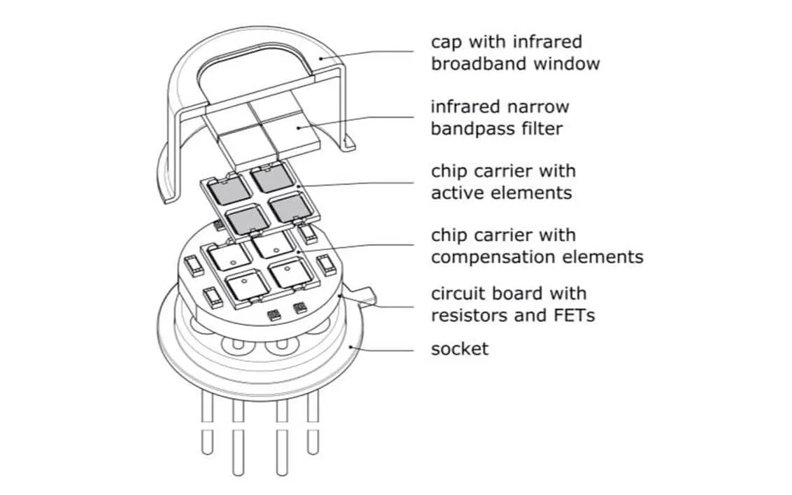
Comparison of detector characteristics
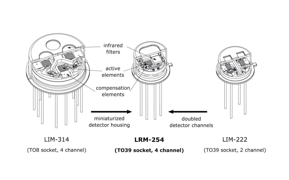
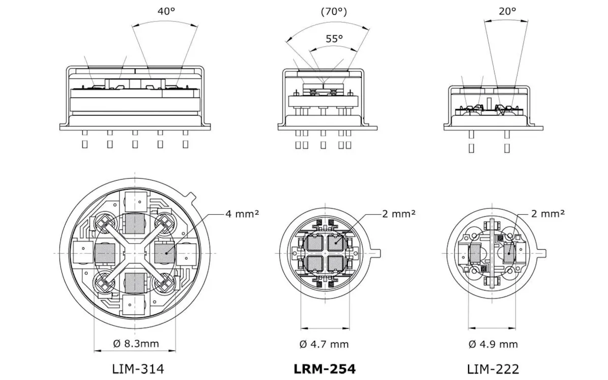
The following section describes the advantages in more detail and quantitatively. The new developed detector LRM-254 is compared with standard detectors LIM-314 (four-channel, TO8) and LIM-222 (dual-channel, TO39) from InfraTec [3]. Fig. 5 shows all three detector types, Fig. 6 illustrates the different optical properties and important parameters are pointed out in Tab. 1.
High integration density
The significantly higher integration density of the LRM-254 becomes apparent in comparison with LIM-222. By having nearly the same active element area (~ 2 mm²) and compensation elements, it is now possible to realize four instead of only two channels. So far that was only possible for TO8 housings (e.g. LIM-314) but with larger sensor elements having up to 4 mm² active area.
Another advantage of the improved integration density is the reduction of the illuminated area and thus the utilization of space. Fig. 6 shows the degree of filling, which describes the ratio of the active sensor element area to the complete illuminated area. The degree of filling for the LRM-254 amounts 40% within a diameter of 4.7 mm. The illumination occurs with a significantly lower loss compared to the standard detectors.
Optimized Field of View
The layout of the newly developed chip carriers was especially adapted to the requirements of a large FOV. This results in the small footprint of the carrier as well as the optimized distance between the mounted pyroelectric elements and the infrared filter above. As shown in Fig. 6, the LRM-254 has a 2.5x higher FOV than the LIM-222 with the same housing but double the number of channels.
Protection of sensitive infrared filters
As mentioned above, the newly developed detectors have a broadband infrared window, which is mounted into the cap. A protection of the sensitive infrared filters against environmental impacts results. Additional to that it is also possible to solder the window instead of adhesive bonding to protect the filters against penetrating humidity.
Tab. 1: Comparison electro-optical properties standard detectors and LRM-254
Cost efficient manufacturing process
The manufacturing of the chip carriers is done by a multistage micro-machining process. A silicon wafer is structured by photolithography and several etching processes. The electrical conductivity is realized by metallization of the wafer. Finally, the wafer is cut to separate chip carriers. Due to the modular design and depending on the required number of channels the carriers can be cut to the appropriate size. It exists three different versions for the following LiTaO
The detector assembly is done by automated die attach and wire bonding processes. The chip carriers can easily be taken from the wafer. Compared to standard detectors, the size of the most costly infrared filters is reduced, causing also a reduction of the material costs.
Summary
Based on a novel micro-machined chip carrier, a new family of miniaturized multi-channel detectors was developed. The concept expands the available degrees of freedom regarding the detector design and opportunities to optimize the detector. The newly introduced LRM-254 (TO39, four-channel) and LRM-202 (TO46, dual-channel) are very compact, thermally compensated (uncompensated also possible) voltage mode detectors. They especially meet the needs of space-saving measurement modules for gas analysis. Currently the LRM254 will be expanded by a single supply current mode type (LRM-284) with an integrated operational amplifier, whereby the integration density will be increased again.
References
[1] G. Wiegleb, Gasmesstechnik in Theorie und Praxis: Messgeräte, Sensoren, Anwendungen. Wiesbaden: Springer Vieweg, 2016.
[2] S.G. Porter, A Brief Guide to Pyroelectric Detectors, Ferroelectrics, Vol. 33, 193-206, (1981); doi:10.1080/00150198108008086
[3] InfraTec GmbH; Catalog 2013: Pyroelectric & Multispectral Detectors, Dresden, InfraTec GmbH Infrarotsensorik und Messtechnik, 2013.
Source of the first publication: Open link.
This is an unmodified version of the article.