Electronic / Semiconductor Testing Solution - E-LIT
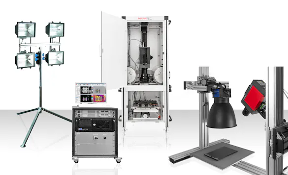
Modular Automated Test Bench
Thermal analysis of electronic and semiconductor devices
Modular test bench for online lock-in measurement
Temperature measurement and Reliable detection of thermal anomalies in the mK and μK range
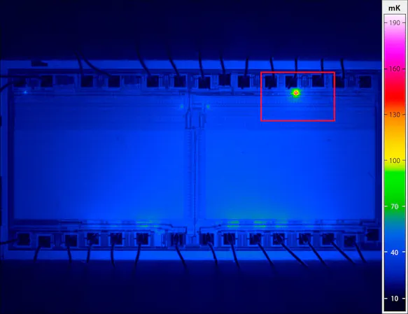
Spatial location of point and line shunts, oxide defects, transistor and diode failures in multilayer PCBs and multi-chip modules
Detection of “watermarks” and thermal signatures for authenticity analysis
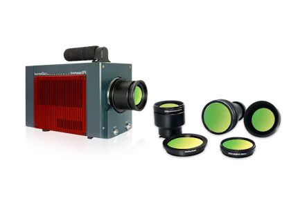
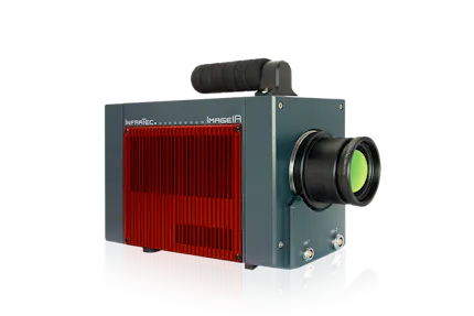
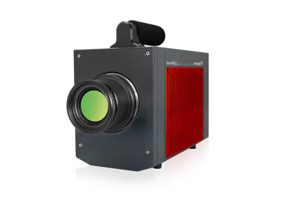
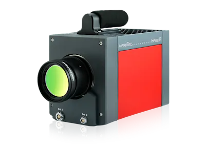
Use of thermographic systems with cooled and uncooled detectors
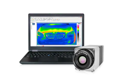
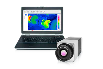
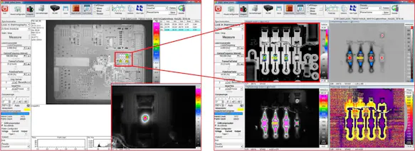
Operational software IRBIS® 3 active for Chip testing with comprehensive analysis options in laboratory conditions

Automated Lock-In measurement with E-LIT from InfraTec

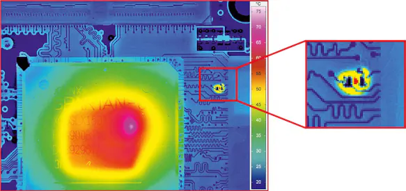
E-LIT – Lock-In Thermography for electronics is an automated testing solution system (as part of NDT techniques) which allows non-contact electrical failure analysis as well as checking the authenticity of semiconductor material, electronic components, and electronic circuits. Inhomogeneous temperature distribution, local power loss, leakage currents, resistive vias, cold joints, latch-up effects and soldering issues can be measured with Lock-in Thermography. This is achieved by using the shortest measurement times combined with a high-performance thermographic camera and a specialised lock-in procedure.
The electrical excitation for the semiconductor test gets its parameters from the system and is clocked with a synchronization module. Even failures that produce mK or even μK temperature differences are reliably detected by the Lock-in Thermography system.
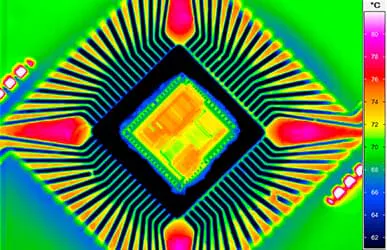
Smallest defects at electronic components like point and line shunts, issues from overheating, internal (ohmic) shorts, oxide defects, transistor and diode failures on a PCB surface, in integrated circuits (IC´s), LED modules and battery cells can be detected and displayed in x and y positions. Additionally, it is possible to analyse stacked-die packages or multi-chip modules in z-direction with merely changing the lock-in frequency. In conjunction with algorithm-based pattern recognition, manipulation of the circuits can also be detected. For these and similar tasks the powerful lock-in thermography software uses the latest algorithms and routines from most recent scientific publications.
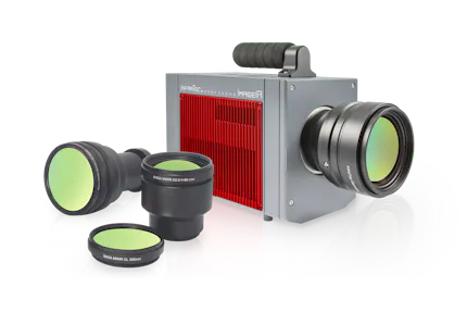
E-LIT is extremely powerful also in resolving the smallest geometrical structures as it can be equipped with strong microscopic lenses and additional SIL lenses. With the help of thermal cameras with detector sizes of up to (2,560 x 2,048) pixels, even micro defects can be recognised and analysed.
Electronics and Semiconductor Module Testing by means of Lock-in Thermography
Find out in our white paper how you can use lock-in thermography to detect faults in electronic and semiconductor components. Benefit from our practical tips and achieve the best possible measurement results with the E-LIT test bench from InfraTec.

Benefits of the Modular Test Bench
Measurement with one workstation - IC failure analysis from the entire circuit board to the smallest detail.
Customised modular measuring station, e. g. with X-Y table and Z-axis manually or motorised adjustable, for positioning and individual adjustment of the working distances, depending on the size of the measured object
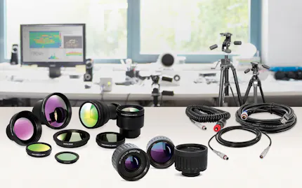
Flexibility through variable components, e.g. different optics, holding devices for the test specimen or contacting options
Online lock-in measurement with the highest sensitivity
Complete and detailed microscopy analysis
Geometrical resolution up to 1.3 μm per pixel with microscope lenses
Thermal resolution in the microkelvin range
High-voltage test station with mandatory contact protection and operating status indicator light
Integration of high-voltage source meter unit up to 3kV
integrated IV curve tracer for i-v characterization
Multi-layer chip testing
Automatic scanning of larger samples due to precision mechanics

Detection and allocation of faults in the µK range
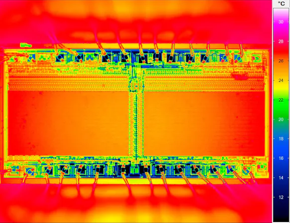
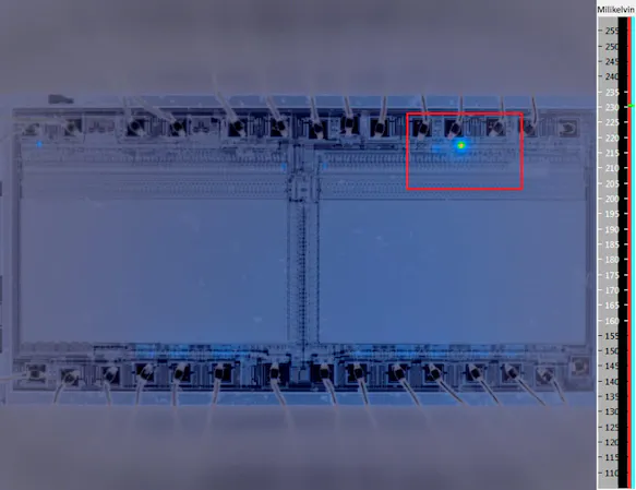
Online Events On Demand: Electronic / Semiconductor Testing Solution
Infrared Lock-in Thermography for Inspection of Electronics and Integrated Circuits
Failure analysis and defect inspection, quality and process control and flexible R&D solution
Hotspot detection on printed circuit boards, integrated circuits, semiconductor material and multi-chip modules
Detection of faulty thermal connections of heat sinks, short circuits, soldering defects and wire bonding errors
Complementary technical lecture Semiconductor IR-LIT Analytics – Challenges and Case Studies from Marko Hoffmann; Infineon Technologies Dresden GmbH & Co. KG
Thermography for Industrial Automation
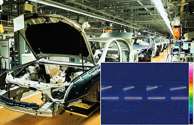
Efficient quality control through fast, contactless temperature measurement during ongoing production
Flexible system solutions from modular components to fully customized turnkey setups
Integrated software for automated evaluation, documentation, and triggering of follow-up processes

Thermographic Images with Different Optics
Telephoto Lens 100 mm
Microscopic Lens 3×
Microscopic Lens 1×

Would You Like to Know More?
It is not unusual for tasks to be associated with special requirements. Discuss your specific application needs with our specialists, receive further technical information or learn more about our additional services.
Thermographic Software IRBIS® 3 active for semiconductor testing
Operational software with comprehensive analysis options in laboratory conditions
Software add-on for automatic failure classification based on parameter settings
Intuitive user interface for easy operation
Real-time display of the electronic object being measured in various states
Multifaceted memory options for image data and measurement results
Alternative 0°, 90° or customised set phase angle image for representation of complex intensity information
Merging live and amplitude image
Optional: IV measurement, under sampling, drift compensation, DC-mode, power loss measurement, user and protocol administration, interface preparation: e.g. Profibus, Ethernet
Product Flyer
Get all the information you need at a glance in our product flyers
